Frontier Sciences: KITA Koji
Formerly, the development of electron devices meant sizing down device elements made of silicon or silicon dioxide. However, minimizing the device structure reached its limit over a decade ago. Consequently, the development goal has shifted to replacing parts of a device with elements made of new high-functional materials. Now, advanced devices are composed of various materials, such as high-mobility semiconductor layers, high-permittivity insular films, and thermally conductive materials installed on silicon wafers. Literary speaking, it is the right “material” in the right place and new materials are the keys to the further advancement of electron devices.
Replacing parts of an electron device with new materials is like suddenly inserting a new external player into a soccer team in which all regular members have been stably fixed in their positions just because the newcomer is an excellent striker. Adding a new material to a conventional device because it has a high efficiency does not simply make the device stronger.
For example, the MOS transistor*1 works when carriers in a semiconductor change their quantity depending on voltage impressed from outside. This performance is made primarily in the domain only one to some tens of nanometers of the interface neighborhood between the semiconductor and the insulator. If demanded property does not appear in this nano domain, the property is useless. However, in the space a length of some atoms from the interfaces, there are various problems: structure distortion, interface reactions or capture of electric charges with dense defect structures (Fig.1). Moreover, dielectric substances scarcely develop on the surface or the interface of materials as demanded.
For a new member to perform effectively in the team, the property control in the nano domain is essential. Therefore, the research requires a knowledge of physics, chemistry, material engineering, and electronics. Research on device materials perfectly matches the concept of the Graduate School of Frontier Sciences: integrating knowledge of various academic fields to approach a research topic.
New materials are not only expected to be used for advanced larger scale integrations or LSIs. In the climate of carbon neutrality endeavor where technology for reducing energy use is heavily emphasized, “wide-bandgap” materials are beginning to be used in power devices*2 (which act as a power convertor), instead of silicon. New materials, such as silicon carbide whose bandgap is three times larger than its of silicon, are especially expected to be applied to big electricity consuming vehicles and facilities; EVs, trains, and large-scale solar power systems, etc. (Fig. 2)
You may be beginning to understand why it is difficult to fully utilize the newcomer’s capacity just by replacing the player at the center forward position. For example, the interface between silicon and a gate insulator film is extremely sensitive. The characteristics of the interface can be completely different depending on whether O2 gas or steam is used for oxidating the silicon carbide surface to make it into a silicon dioxide surface. In addition, inserting one atomic layer of nitrogen improves the interface quality.
Silicon-carbide power devices are widely used now for trains and other vehicles. It is apparently more efficient than silicon devices. However, silicon-carbide devices still have much more potentials, and research is still in its infancy. The new phase of research for developing the supreme power device has just started. Based on material science, we are trying to create the next generation technology in our laboratory (Fig.3) Please look forward to a tremendous advancement of power devices’ efficiency in the near future.
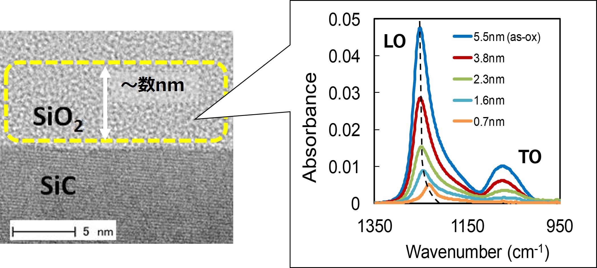


(Fig. 1)
The interface of a wide-bandgap semiconductor and a gate insulator of SiO2 (left) and its structure analysis by infrared spectroscopy (right).
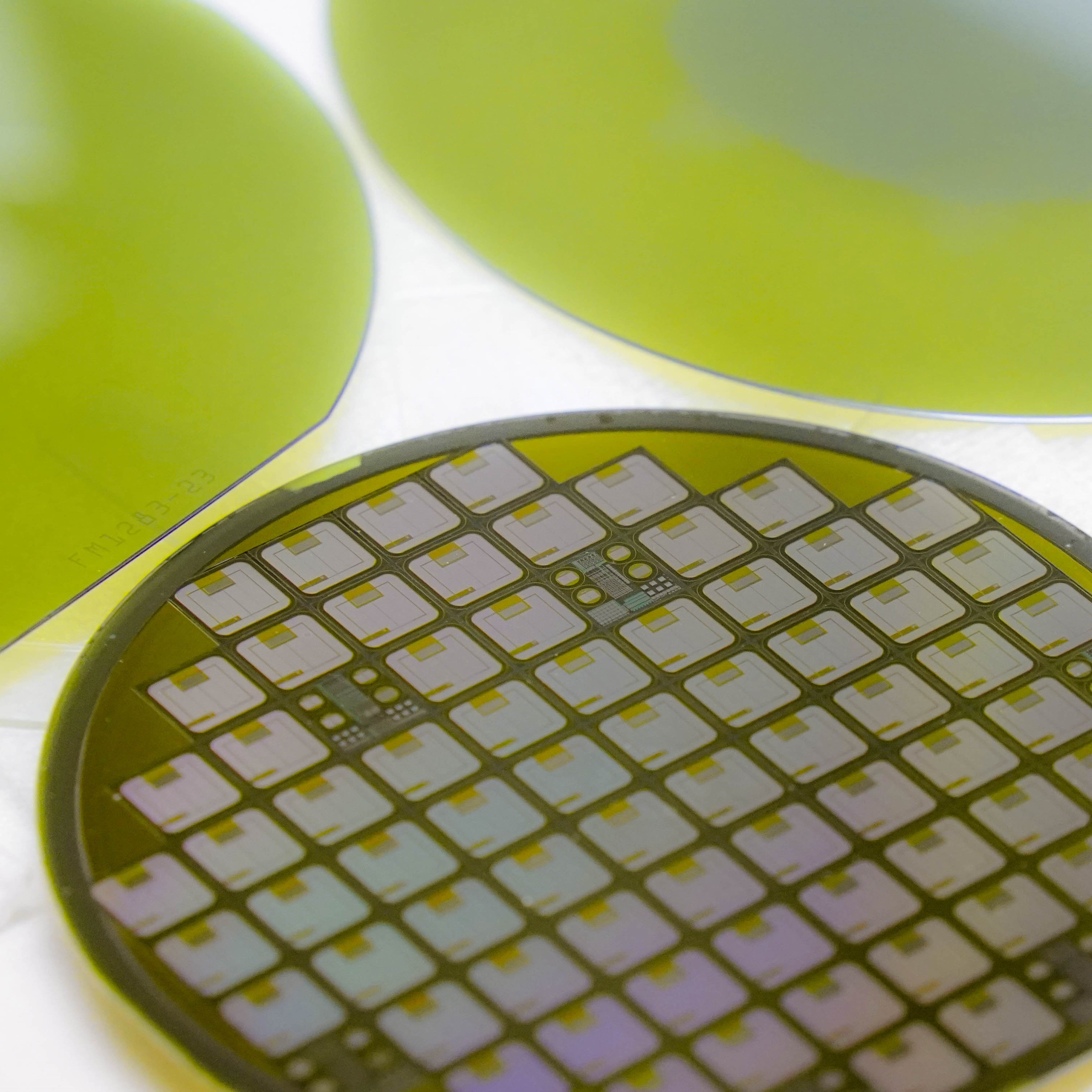
(Fig. 2)
SiC is expected to be a power device of the next generation.
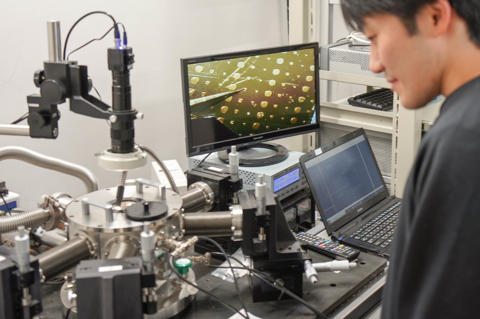
(Fig. 3)
Checking the characteristics of a prototype device
*1 MOS transistor:
Metal-oxide-semiconductor field-effect transistor is a device for the semiconductor surface to either allow the electricity flow or block the electricity by applying voltage between a metal electrode and a semiconductor, sandwiching in an insulator, to induce electric charges.
*2 Power device:
A general term for devices that convert AC/DC and frequency of AC by modulating electricity in the device.
KITA Koji
Professor
Division of Transdisciplinary Sciences
Nano-Space Function Design
Group of Materials Design and Processing
Department of Advanced Materials Science
vol.40
- Cover
- Feature Article: The Forefront of VR - POSSIBILITY OF HAPTICS
- Material Science: The Driver of Electron Device Evolution
- Floating Platform for Sustainable System
- GSFS FRONTRUNNERS
- Voices from International Students
- ON CAMPUS x OFF CAMPUS
- EVENT & TOPICS
- Awards
- INFORMATION
- Relay Essay: School in Switzerland