INTRODUCTION OF LABORATORY

To improve the performance of today’s electron devices dramatically, it is essential to incorporate new device materials with higher functionality. In the electron device operations, the carrier density change in semiconductors occurs in the near-interface region within several or tens of nanometers of the interface between the semiconductor and the insulating layer. Therefore, in order to fully utilize new device materials, it is essential to control the atomic arrangement and physical properties in this nano-region near the interface, by designing appropriate fabrication processes based on the deep understanding of the properties of those materials. For example, it is contributing to an energy-saving society to signicantly improve the efciency of power devices for electric power conversion, by fully utilizing wide-gap semiconductors instead of Si as the new device material. The materials showing superior dielectric properties such as ferroelectricity in nanometer-thick lms, are expected to be applied to new non-volatile memory technology that will support the next-generation computing.

KEN-ICHI UCHIDA LAB. research


バルク材料合成技術や薄膜作製技術を駆使して自然界には存在しない複合材料を生み出し、高効率に熱変換・熱制御・熱移送するための基盤原理・技術を構築しています。

KEN-ICHI UCHIDA LAB. research


本研究室が開発した「熱電永久磁石」の写真。この材料は永久磁石でありながら、電流を流すと電流と直交した方向に熱流が流れて片面を冷却したり、温度差を与えることで発電したりすることができます。

Message

Discover and observe phenomena by ourself and lay the foundation for new research fields. Let's create world-leading research from Japan.

Ever since I was a child, my parents never told me to do anything and I decided on my carrier by myself including the selection of the university. In fact, I never once thought of becoming a researcher until I started my research. I chose to be a researcher because I found that I like doing research.
The field of spin caloritronics has developed from a physical phenomenon I discovered when I was an undergraduate student in Keio University. This is a field that offers great opportunities for students to play an active role. Currently, we are working not only on basic research, but also on how to evelop the various principles discovered in spin 
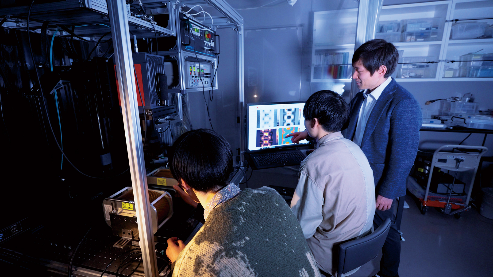
caloritronics for practical applications. Our laboratory conducts research in cooperation with Spin Caloritronics Group, Research Center for Magnetic and Spintronic Materials, National Institute for 
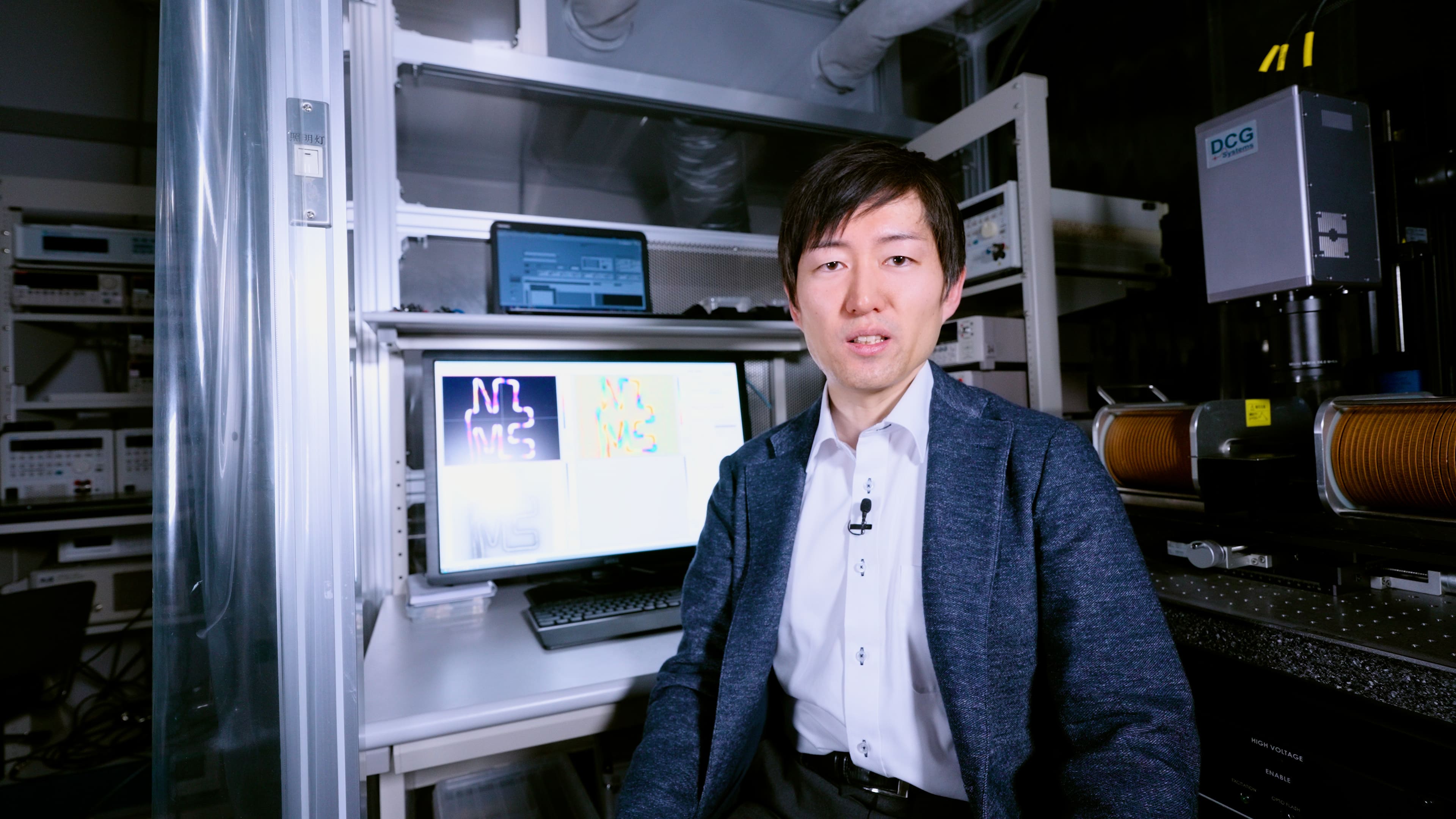
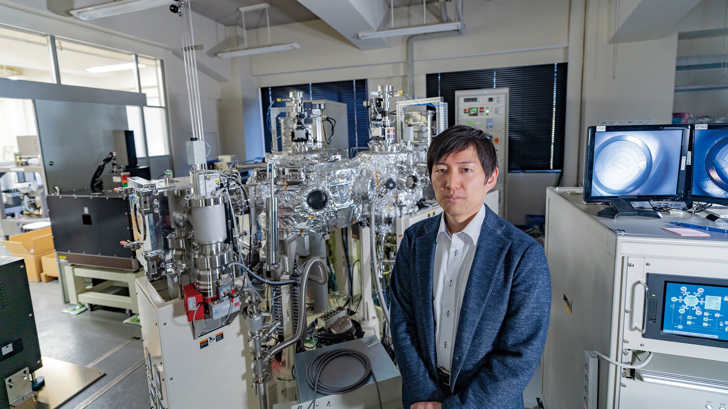
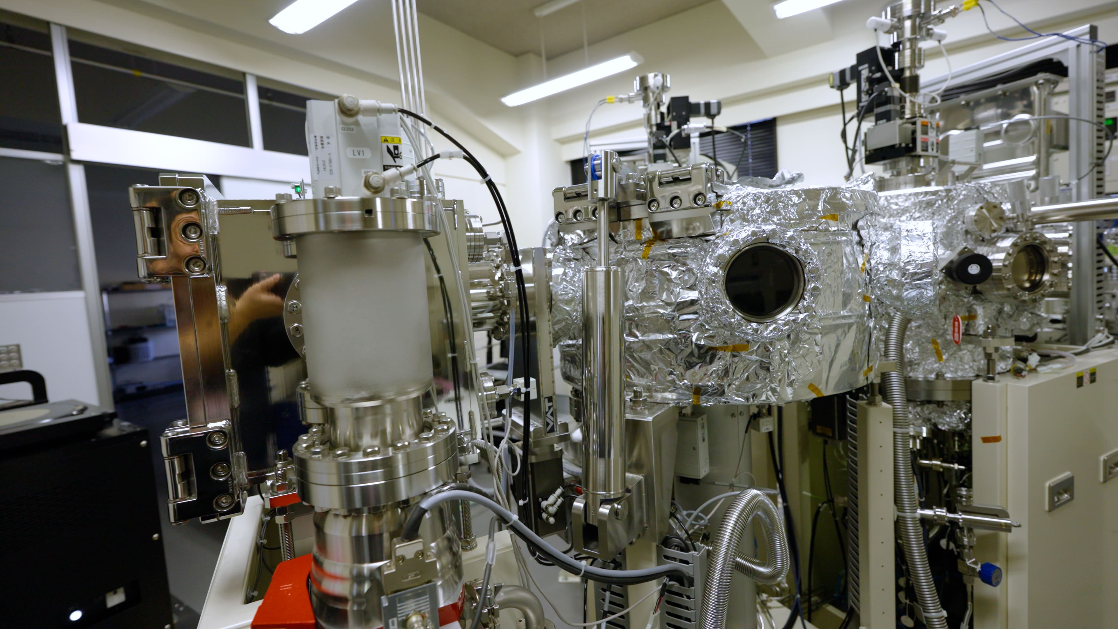
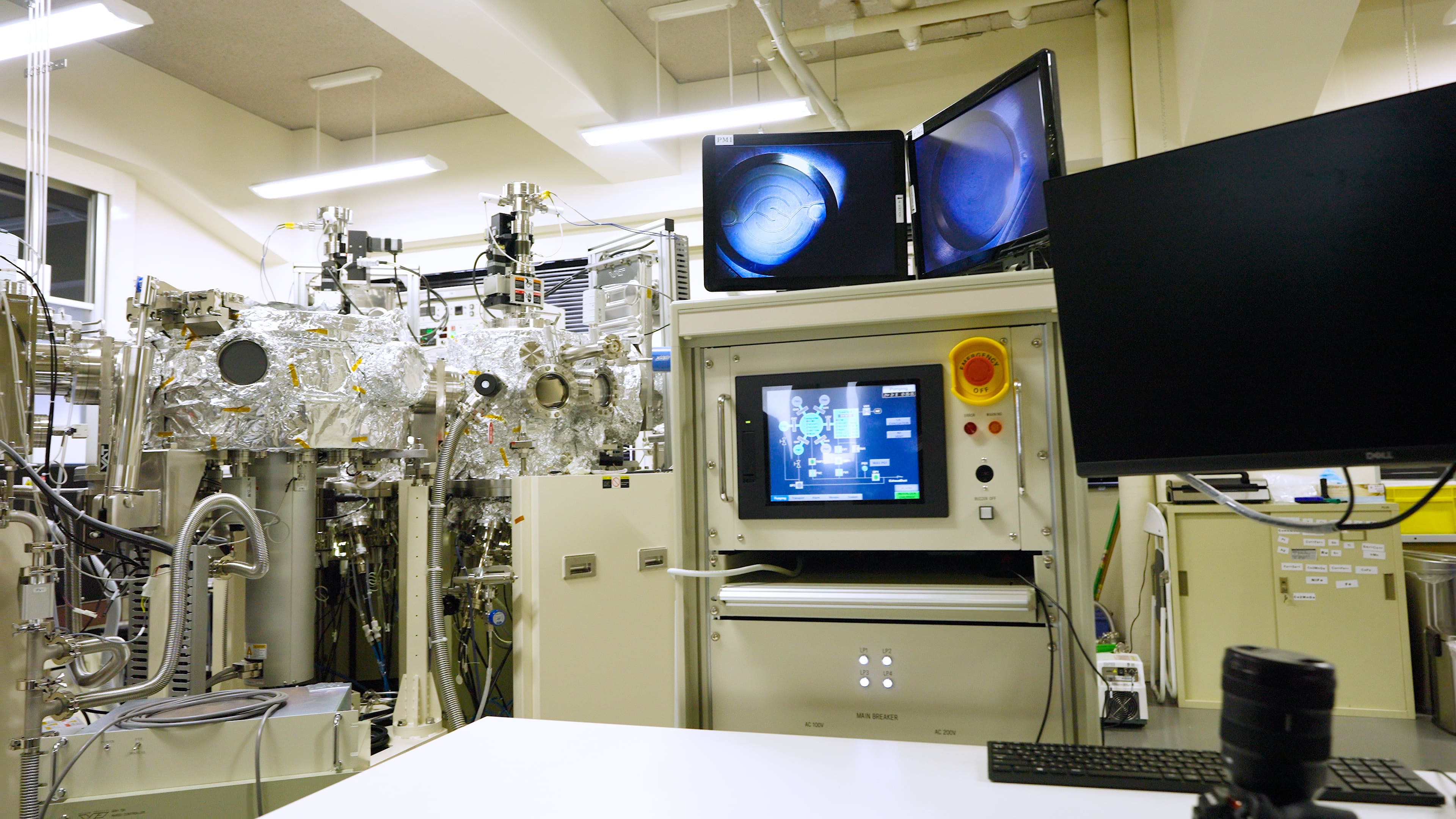
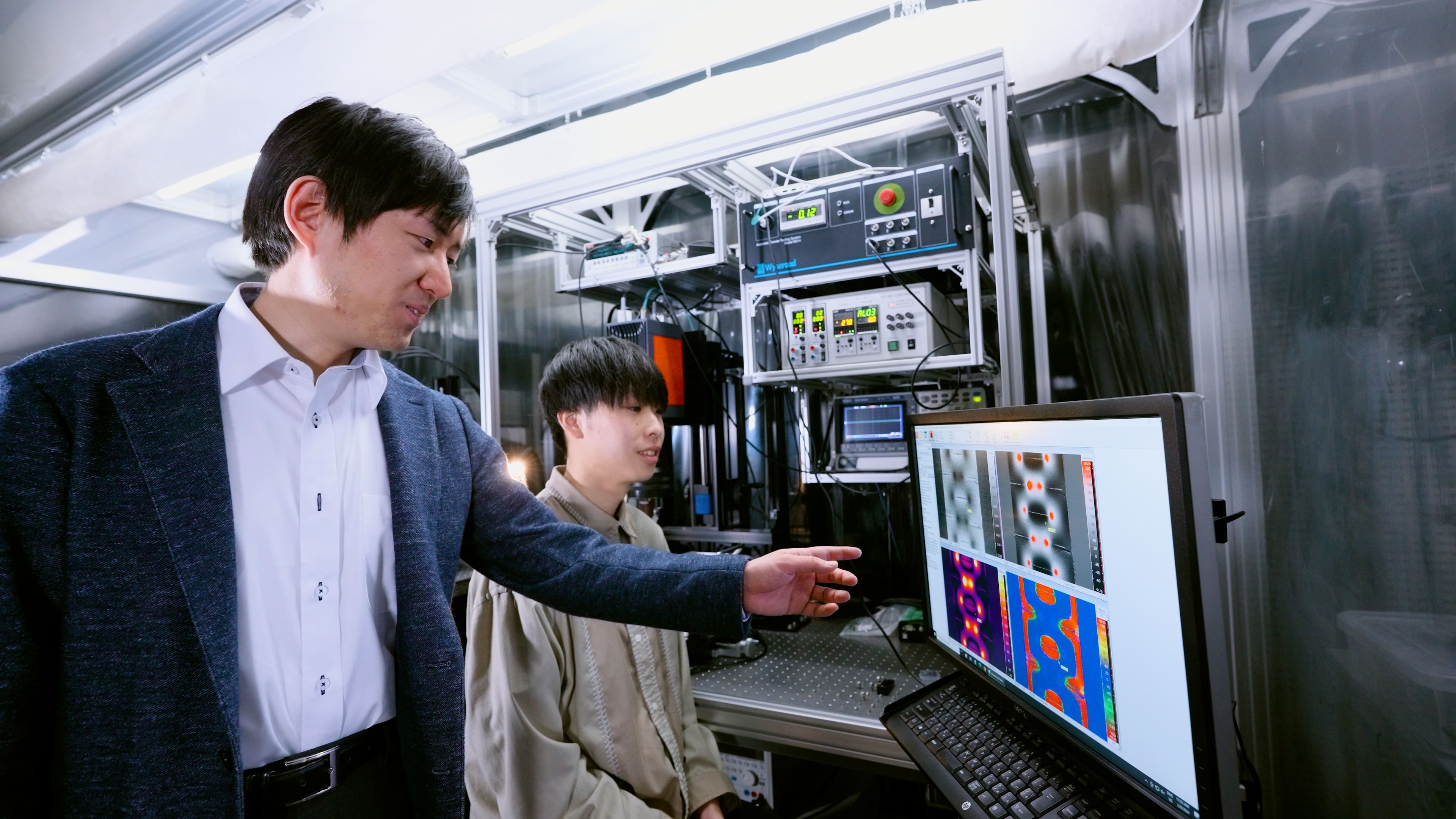
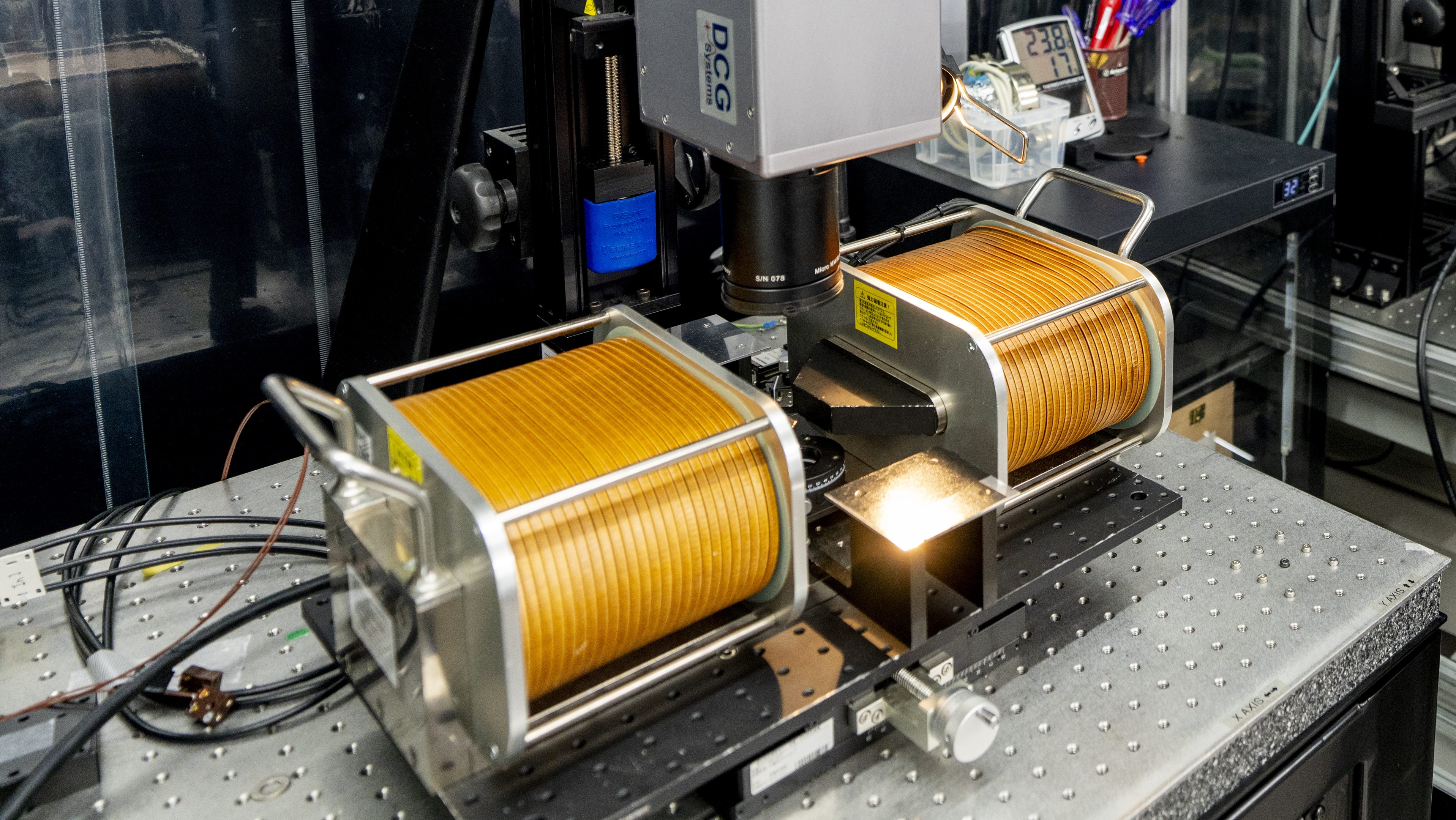
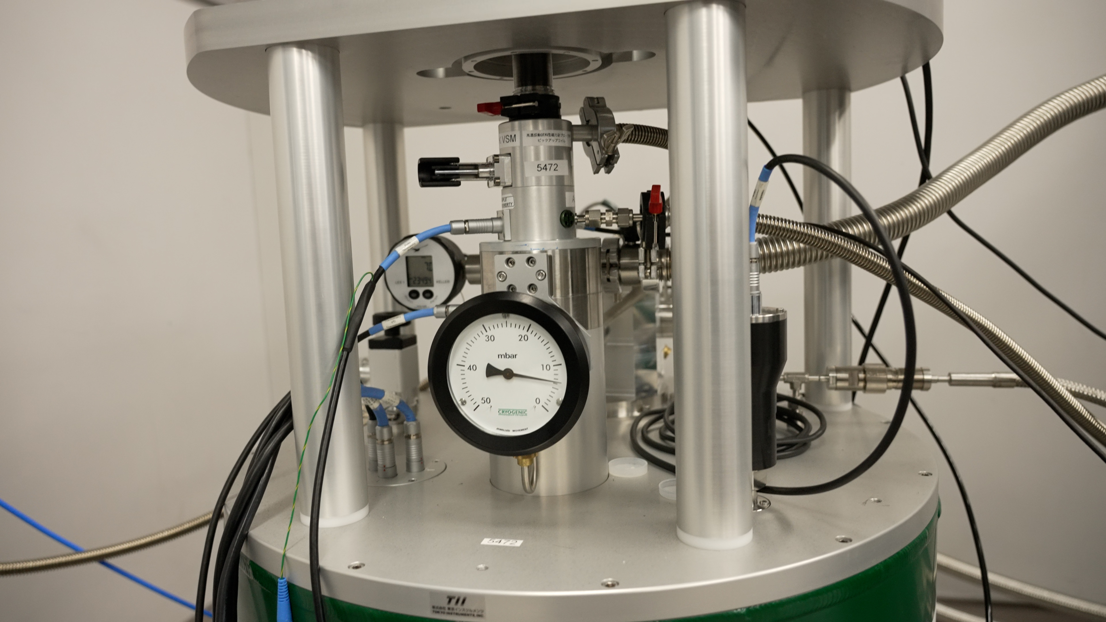
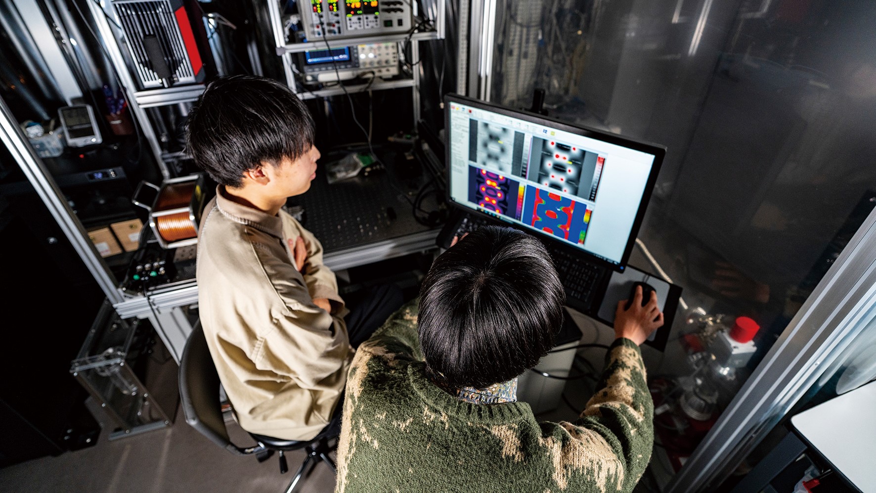
Materials Science (NIMS) in Tsukuba. Students in this laboratory can use state-of-the-art facilities not only at Univ. Tokyo but also at NIMS.

PROFILE

Professor Ken-ichi Uchida

Professor Ken-ichi Uchida

2008 B. Eng., Keio University, Japan

2009 M. Sc. Eng., Keio University, Japan

2012 Ph.D. (Physics), Tohoku University, Japan

2012 Assistant Professor, Institute for Materials Research, Tohoku University

2014 Associate Professor, Institute for Materials Research, Tohoku University

2016 Group Leader, Research Center for Magnetic and Spintronic Materials, National Institute for Materials Science

2023 Distinguished Group Leader, Research Center for Magnetic and Spintronic Materials, National Institute for Materials Science

2024 Professor, Graduate School of Frontier Sciences, The University of Tokyo

Visiting laboratory

  • +81-4-7136-3756(Kashiwa)
  • +81-29-859-2062(NIMS)
  • Ken-ichi UCHIDA Lab.,
  • Department Of Advanced Materials Science,
  • Graduate School of Frontier Sciences,
  • The University of Tokyo
  • Kashiwanoha 5-1-5,
  • Kashiwa,Chiba 277-8561, Japan
  • kuchida@edu.k.u-tokyo.ac.jp