INTRODUCTION OF LABORATORY

To improve the performance of today’s electron devices dramatically, it is essential to incorporate new device materials with higher functionality. In the electron device operations, the carrier density change in semiconductors occurs in the near-interface region within several or tens of nanometers of the interface between the semiconductor and the insulating layer. Therefore, in order to fully utilize new device materials, it is essential to control the atomic arrangement and physical properties in this nano-region near the interface, by designing appropriate fabrication processes based on the deep understanding of the properties of those materials. For example, it is contributing to an energy-saving society to signicantly improve the efciency of power devices for electric power conversion, by fully utilizing wide-gap semiconductors instead of Si as the new device material. The materials showing superior dielectric properties such as ferroelectricity in nanometer-thick lms, are expected to be applied to new non-volatile memory technology that will support the next-generation computing.

YOSHIHIKO OKAMOTO LAB. research


ワイドギャップ半導体SiCのMOSFET反転層移動度のアニール処理による向上効果

YOSHIHIKO OKAMOTO LAB. research


ワイドギャップ半導体SiCとゲート絶縁膜SiO2の界面と、赤外分光による構造解析

岡本研究室 研究紹介


CaAgPにおいて実現した、「ノーダルライン半金属」と呼ばれる珍しい電子構造。Pdを添加したCaAgP単結晶の電気抵抗は、磁場中で特異な振る舞いを示した。

Message

What is the most meaningful study to develop the technologies for the future society? That was the reason why I started to learn materials science. In the world of electron devices, “things we hope to do" are changing to “things we can do” every day.

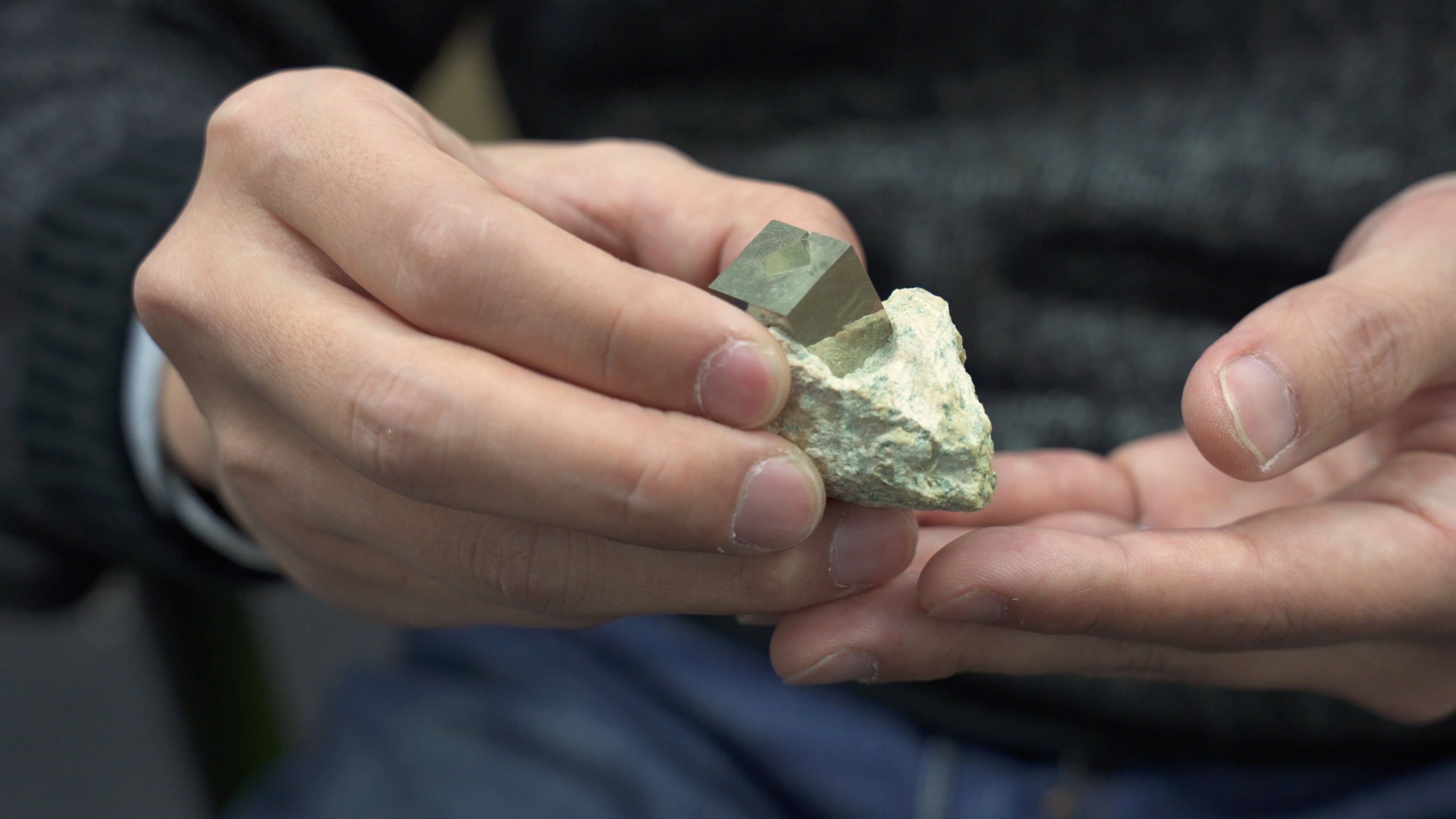
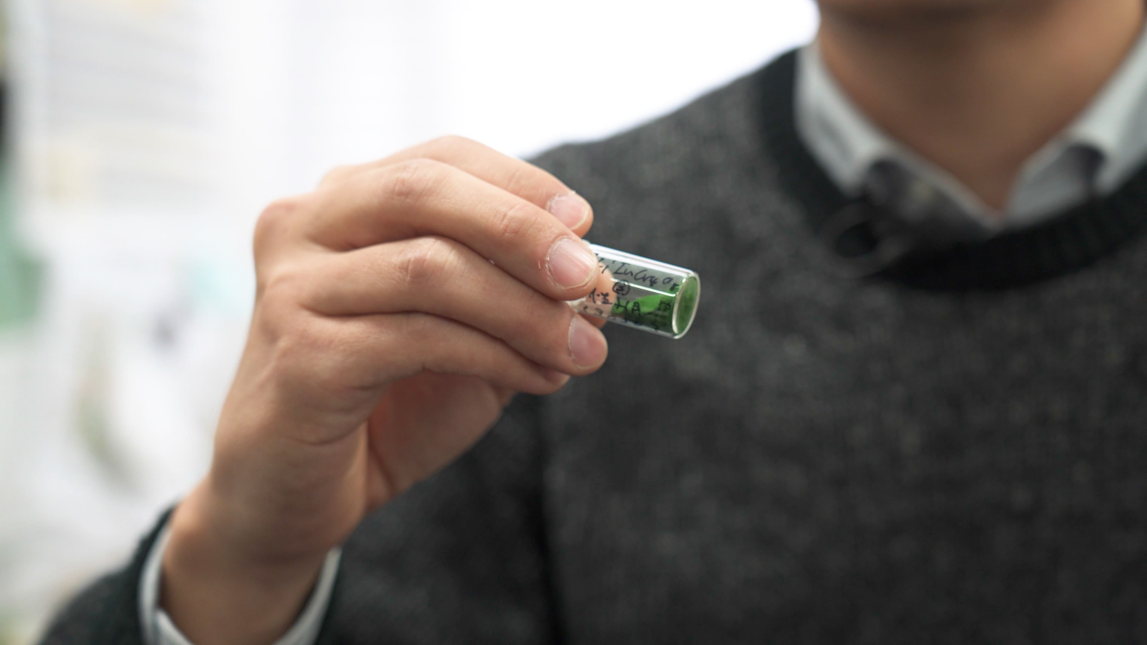
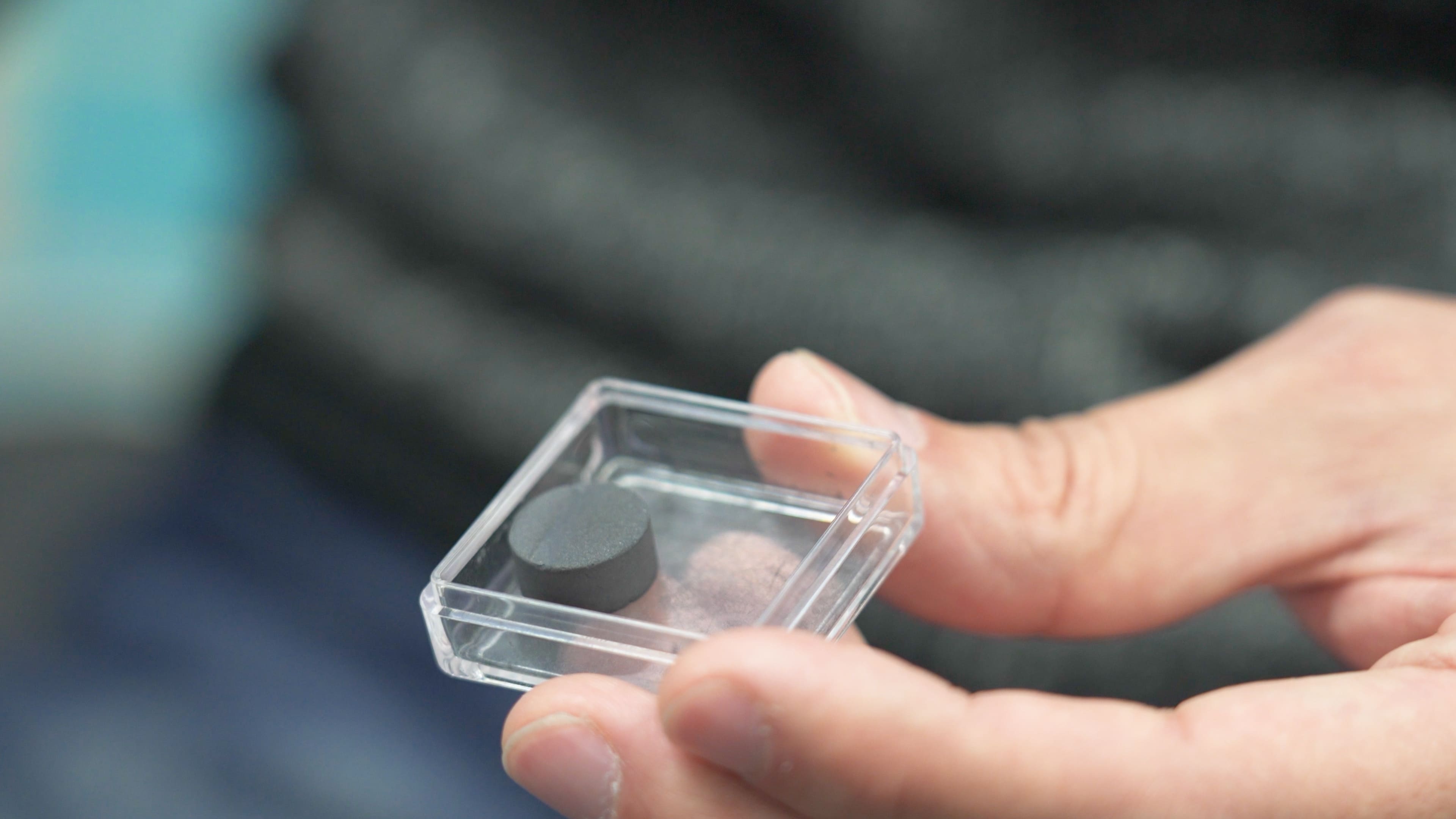
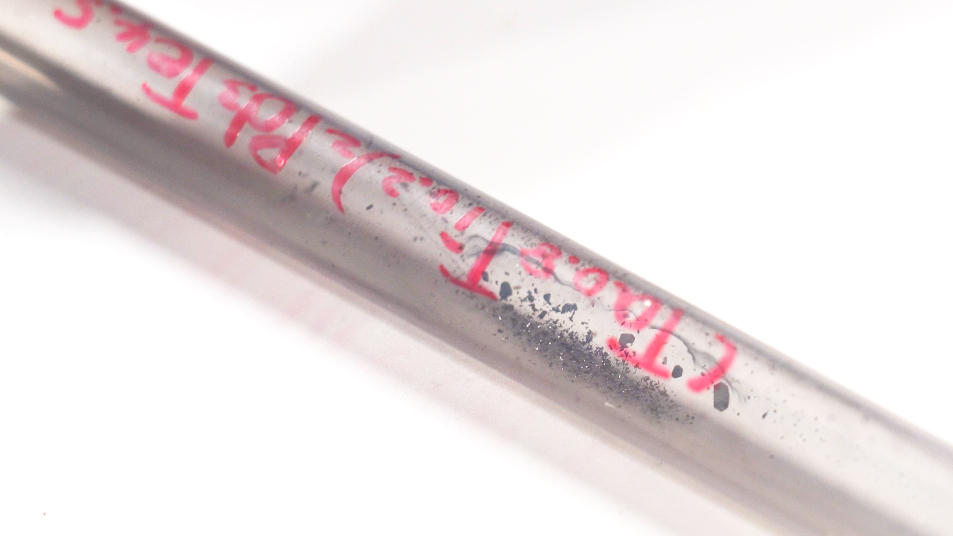
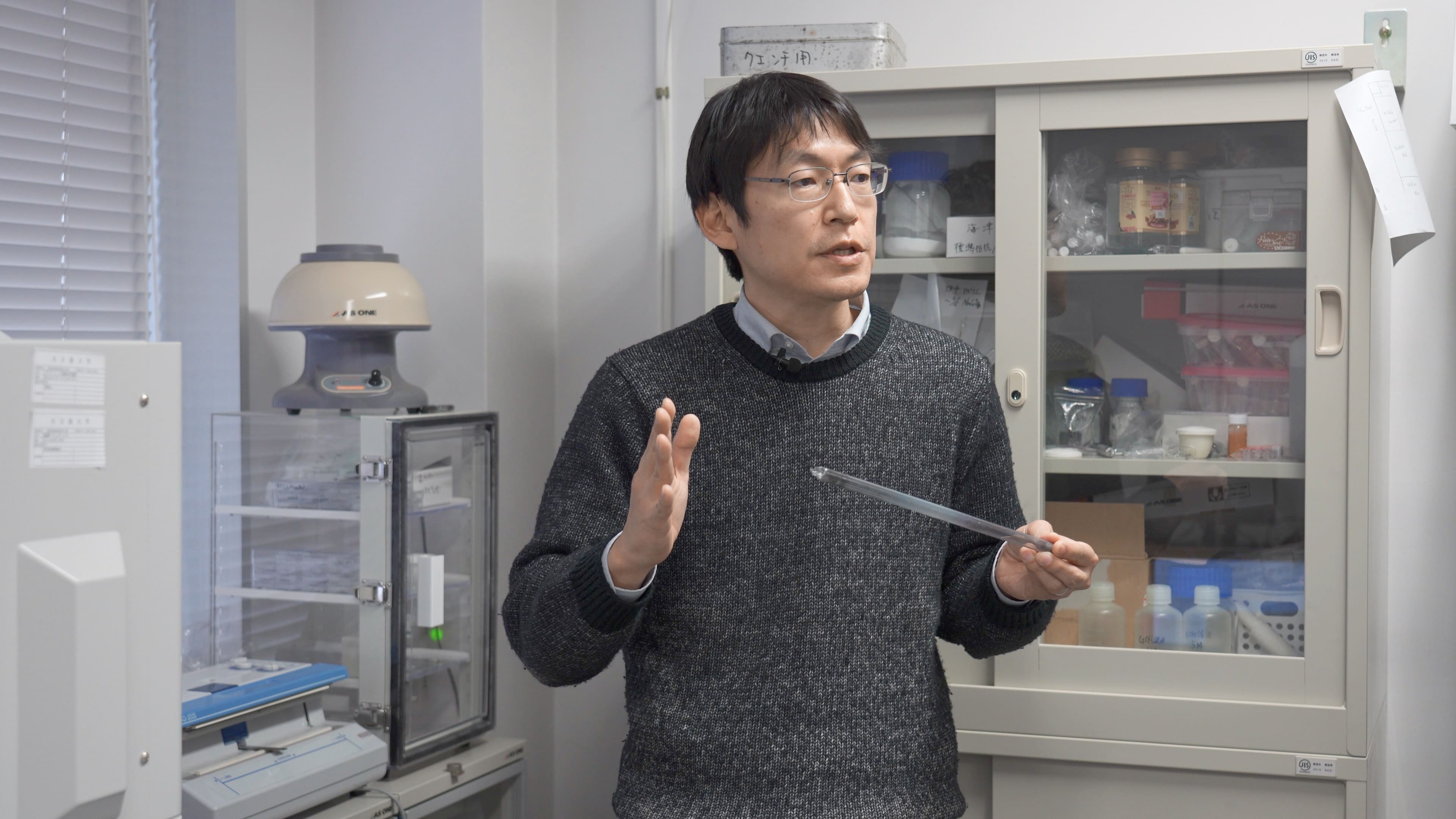
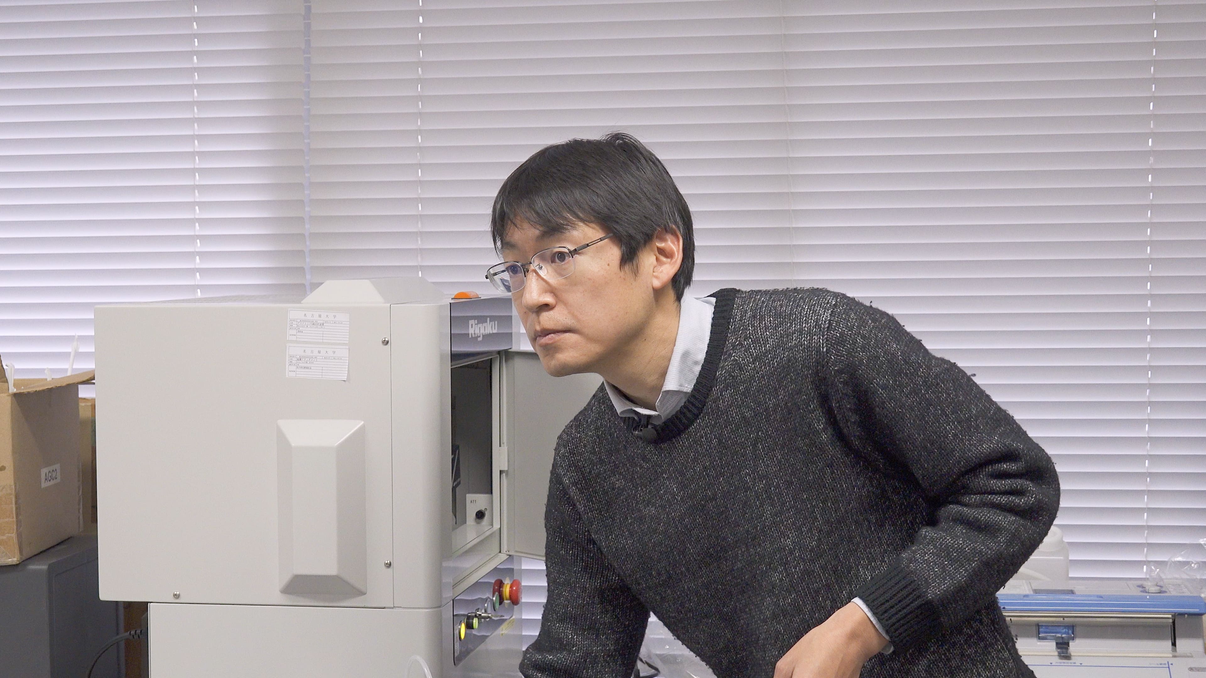
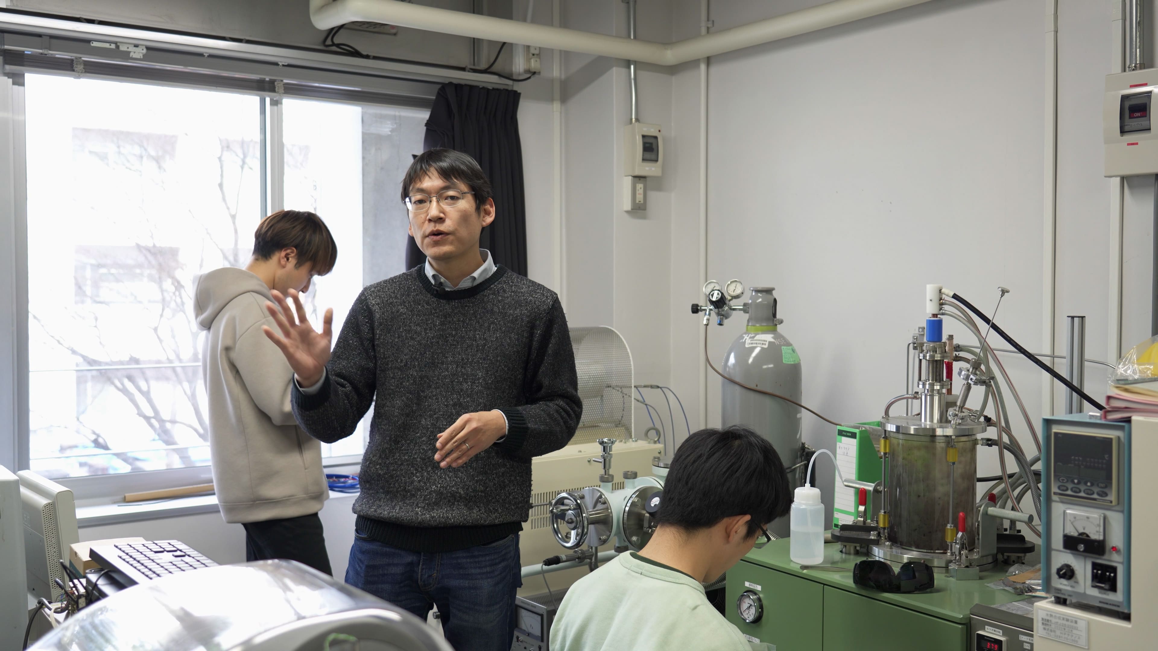
I majored in chemical engineering because learning chemis-try seemed necessary to understand the technology for the benet of our society, such as the technologies for environ-mental conservation and efcient usage of energy. After graduation, I started to work with a professor leading the cutting-edge research on electron devices with in-depth knowledge of physics. While I kept struggling to pursue his many creative ideas, I nally found my way to come to where I am today. Today materials science provides one of the keys for develop-ing advanced electron devices. In this research eld, special-ists in materials science are not the majority, so I always feel I am responsible for the role to clarify the technological issues in device physics from a perspective of materials science. In those researches, we cannot nd a solution without repeat-ing trials to test our various ideas over and over again. That is how future technology develops. We should enjoy such struggling to keep moving the technology forward.

PROFILE

Professor Yoshihiko Okamoto

Professor Yoshihiko Okamoto

2001-2006 Department of Advanced Materials Science, University of Tokyo, Dr. Sci.

2006 Special Postdoctoral Researcher, RIKEN

2006-2014 Research Associate, Institute for Solid State Physics, University of Tokyo

2014-2022 Associate Professor, Department of Applied Physics, Nagoya University

2014-2018 Associate Professor, Institute for Advanced Research, Nagoya University

2018-2019 Visiting Associate Professor, Institute for Chemical Research, Kyoto University

2018-2022 Specially Appointed Associate Professor, Institute of Innovative Research, Tokyo Institute of Technology

2022 Professor, Institute for Solid State Physics, University of Tokyo

Visiting laboratory

  • +81-4-7136-3250
  • Yoshihiko Okamoto Lab.,
  • Department Of Advanced Materials Science,
  • Graduate School of Frontier Sciences,
  • The University of Tokyo
  • Kashiwanoha 5-1-5,
  • Kashiwa,Chiba 277-8561, Japan
  • yokamoto@issp.u-tokyo.ac.jp